
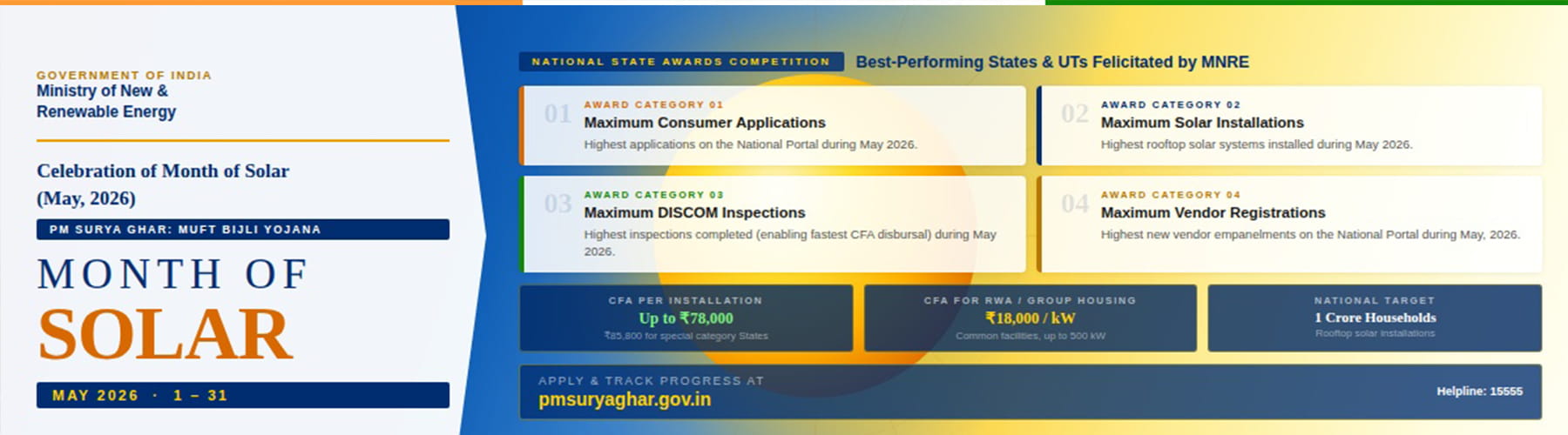
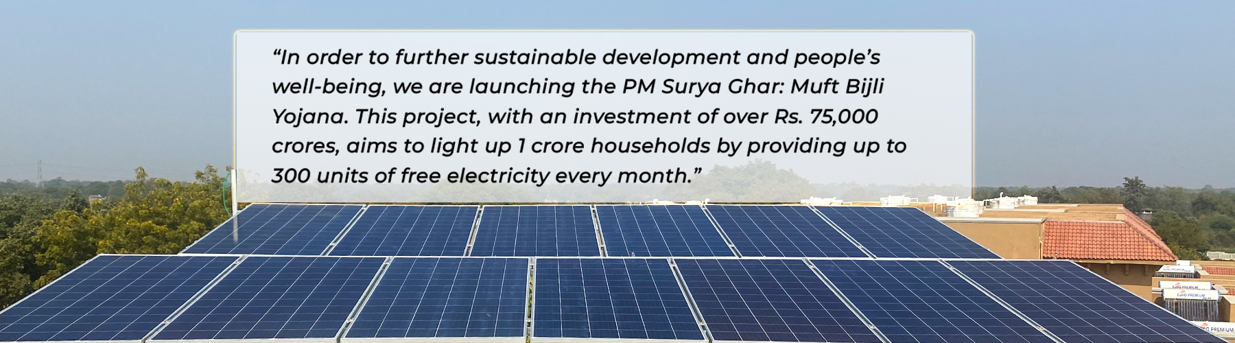
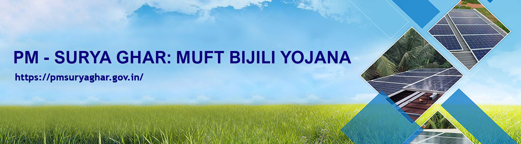
पीएम – सूर्य घर : मुफ्त बिजली योजना


(माननीय कैबिनेट मंत्री)
(माननीय राज्य मंत्री)
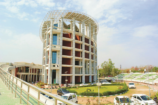
राष्ट्रीय सौर ऊर्जा संस्थान (नाईस), नवीन और नवीकरणीय ऊर्जा मंत्रालय (एमएनआरई) का एक स्वायत्त संस्थान है, जो सौर ऊर्जा के क्षेत्र में अनुसंधान और विकास के लिए एक शीर्ष संस्थान है।
नवीन और नवीकरणीय ऊर्जा मंत्रालय (एमएनआरई) भारत सरकार द्वारा वर्ष 1998 में चेन्नई में स्थापित एक स्वायत्त अनुसंधान और विकास संस्थान है।
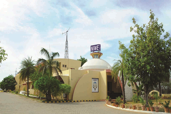
सरदार स्वर्ण सिंह राष्ट्रीय जैव ऊर्जा संस्थान (एसएसएस-नीबे), कपूरथला (पंजाब) नवीन और नवीकरणीय ऊर्जा मंत्रालय का एक स्वायत्त संस्थान है।
भारतीय अक्षय ऊर्जा विकास संस्था लिमिटेड (इरेडा), नवीन और नवीकरणीय ऊर्जा मंत्रालय (एमएनआरई) के प्रशासनिक नियंत्रणाधीन एक 'नवरत्न' गैर-बैंकिंग वित्तीय संस्थान है। इरेडा मुख्य रूप से परियोजनाओं की स्थापना को बढ़ावा देने, उनका विकास करने और वित्तीय सहायता प्रदान करने में शामिल है।
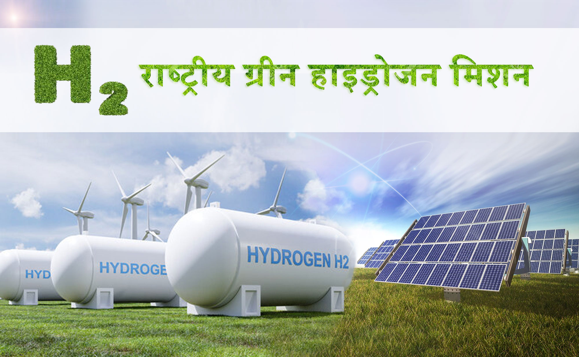
नवीन और नवीकरणीय ऊर्जा मंत्रालय (एमएनआरई) के अंतर्गत एक अनुसूची-क केन्द्रीय सार्वजनिक क्षेत्र का उपक्रम (सीपीएसई) है, जो भारत और विदेशों में अक्षय ऊर्जा परियोजनाओं (सौर, पवन, हाइब्रिड, चौबीसो घंटे अक्षय ऊर्जा, हाइड्रोजन आदि) का कार्यान्वयन और विकास कर रहा है।
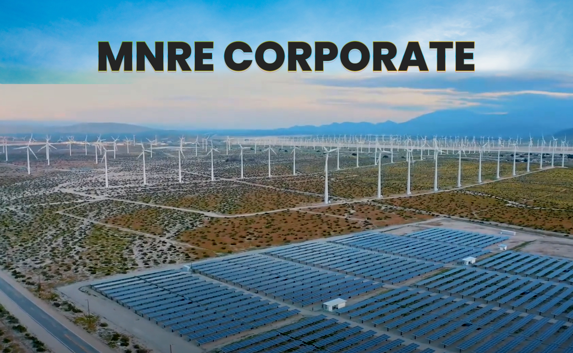
नवीन एवं नवीकरणीय ऊर्जा मंत्रालय (एमएनआरई) देश में ग्रिड-कनेक्टेड और ऑफ-ग्रिड नवीकरणीय ऊर्जा को बढ़ावा देने के लिए केंद्रीय स्तर पर नोडल एजेंसी है। मंत्रालय के कार्यक्रम नवीकरणीय ऊर्जा (आरई) के लिए राज्य नोडल एजेंसियों (एसएनए) के साथ निकट समन्वय में कार्यान्वित किए जाते हैं।
अंतर्राष्ट्रीय सौर गठबंधन, विभिन्न सरकारों के बीच एक संधि आधारित संगठन है, जिसका लक्ष्य सौर ऊर्जा के व्यापक विकास के लिए वर्ष 2030 तक आवश्यक 1000 बिलियन यूएस डॉलर जुटाना है। भारत के प्रधान मंत्री श्री नरेन्द्र मोदी और फ्रांस के राष्ट्रपति श्री फ्रॉंस्वा ओलांद द्वारा 30 नवम्बर, 2015 को स्थापित ISA का लक्ष्य सौर वित्तपोषण, टेक्नोलॉजी, इनोवेशन, अनुसंधान और विकास तथा क्षमता निर्माण के लिए मांग जुटाकर सौर ऊर्जा और विद्युत का उत्पादन बढ़ाना तथा उत्पादन की लागत में कमी लाना है।
और पढ़ें